STM32F0 Discovery Kit hack saw hack
Two dev boards for the price of one
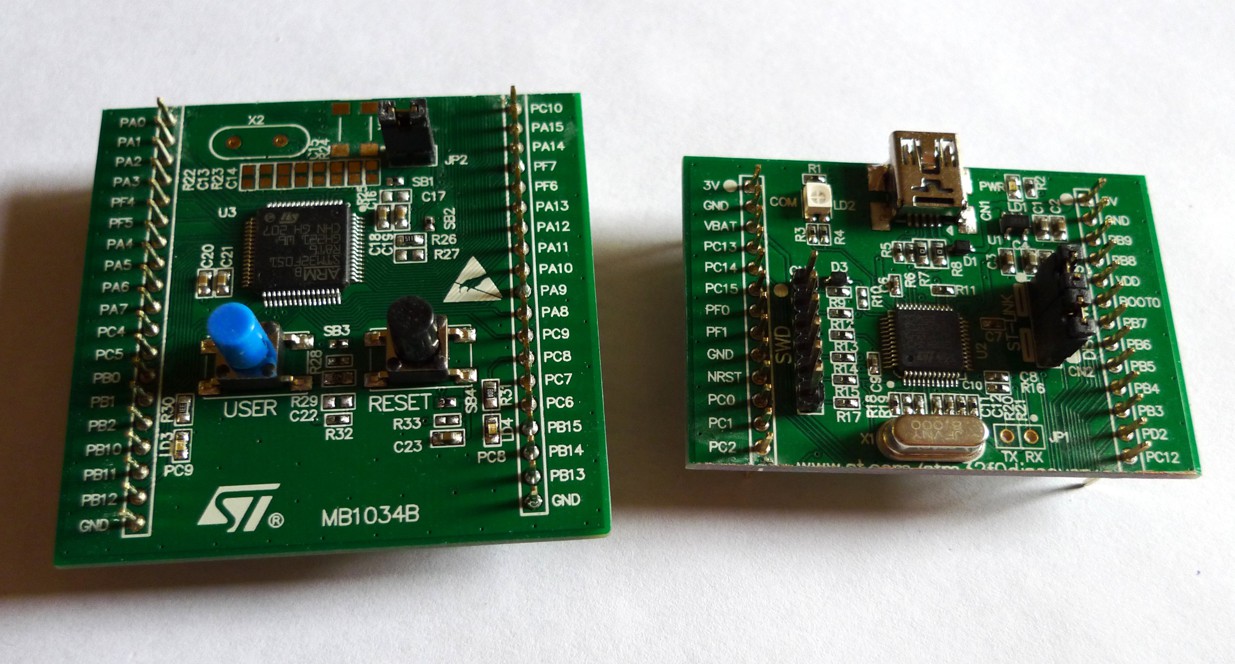
I recently picked up a delightful STM32F0 Discovery Kit which, even from the supplier that rhymes with “Darnell”, was really cheap – about £7 inc. VAT:
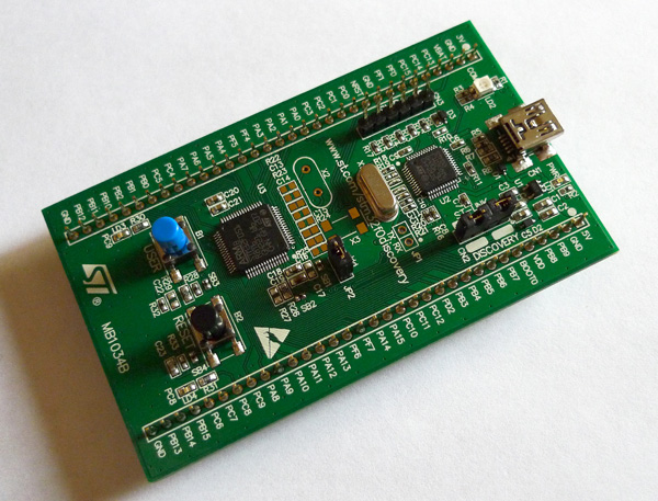
The centre of attention is the STM32F0 chip on the left. These are good fun! 8K RAM and 64K flash, an ARM Cortex-M0 running at 48MHz (powerful!), decent fast ADCs and various other useful peripherals. I think I’m going to leave AVRs behind…
However, to make it nice and easy to program out of the box, the board also contains a “ST-LINK v2” USB-to-Serial Wire Debug module (on the right). This consists of a STM32F103 ARM Cortex-M3 microcontroller (20K RAM, 64K flash and 72MHz), more powerful than the -M0!
I had a project in mind for the M0 but the board was far too large for the enclosure I had planned. Since the ST-LINK has headers to program an external uC, I figured I could cut out the M0 portion (sized for my project) and use the programmer half separately, via flywires. This then provides the option of programming any other board, including programming the programmer of a second similarly-sawn board!
Under the knife:
Preparation time: 10 minutes.
Cooking time: 10 minutes.
You will need:
- An STM32F0 DK
- A soldering iron
- A hacksaw with a fine blade, or a bandsaw
- Some sort of common sense with tools and safety
- 0.1” pin sockets (4x1), wire and J-clips
The board is evenly divided into “programmer” and “M0”. I chose to cut at the horizontal line joining pins PC3 and PC11. Obviously you will lose access to the pins on the top half of the board – but the bottom half still has plenty of ADC inputs, SPIs, UARTs available.
1. De-solder pins PC3 & PC11
This will make it easier to guide the saw and save you from having to saw through pins… Cut the black plastic off the bottom then tweezer the pins out when hot.
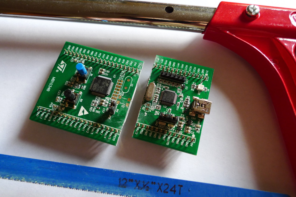
2. Saw the board in half
Have fun! Don’t cut yourself! Try to keep the line between PC3 and PC11 as straight as possible so as not to damage the pins below. The wider the cut the fewer I/Os you have… and try not to hit the crystal on the programmer half!
File the edges until soft.
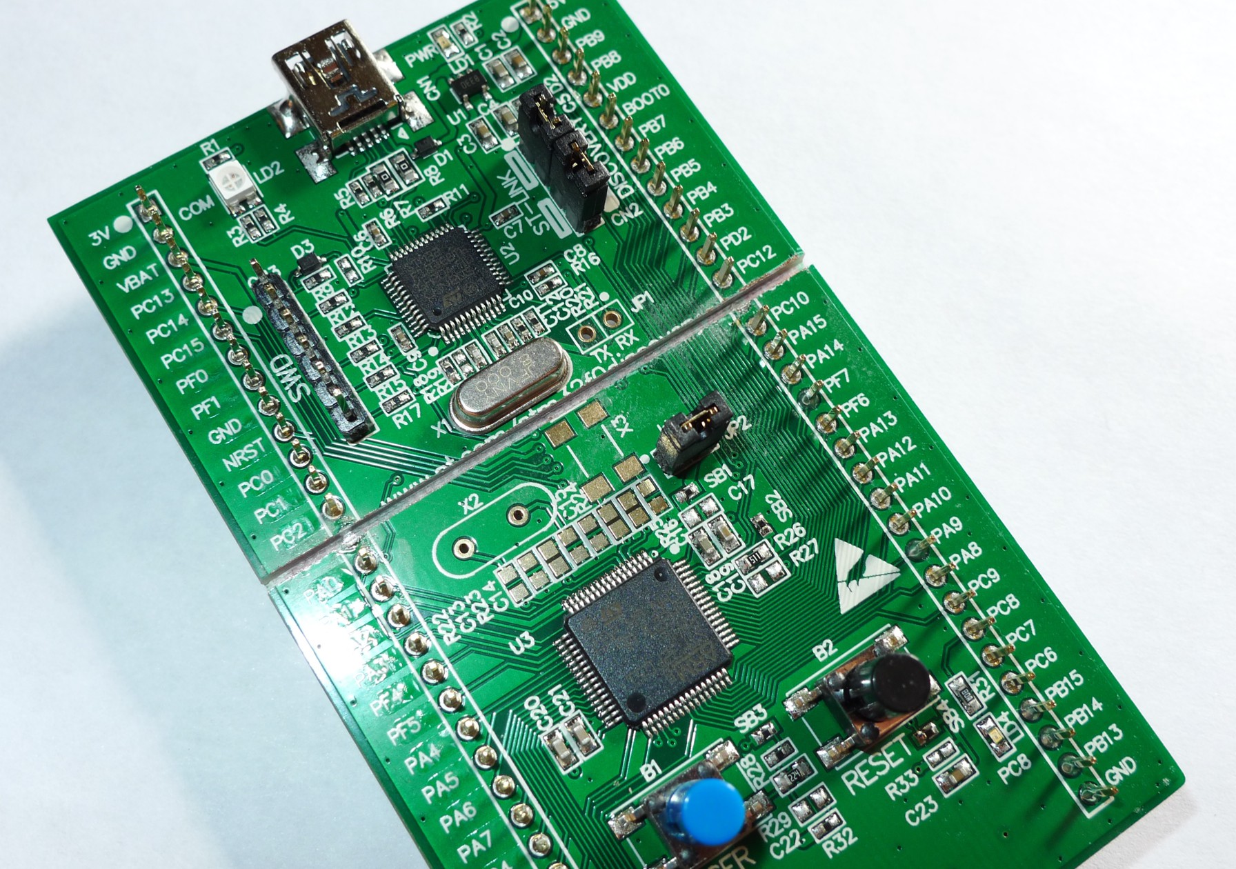
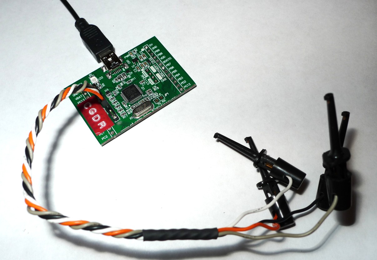
3. Make a cable to plug onto CN3
The programmer half has a connector, CN3, bringing out the Serial Wire Debug signals. We’re interested in SWDIO, SWCLK, nRESET and ground. In the pictures below I have made a 4-wire cable with J-clips that sits on the centre four of the six CN3 pins. Labelling the pins are useful too!
Remove the jumpers on CN2. The six pins on CN3 are:
- 1: NC
- 2: SWCLK
- 3: GND
- 4: SWDIO
- 5: nRESET
- 6: NC
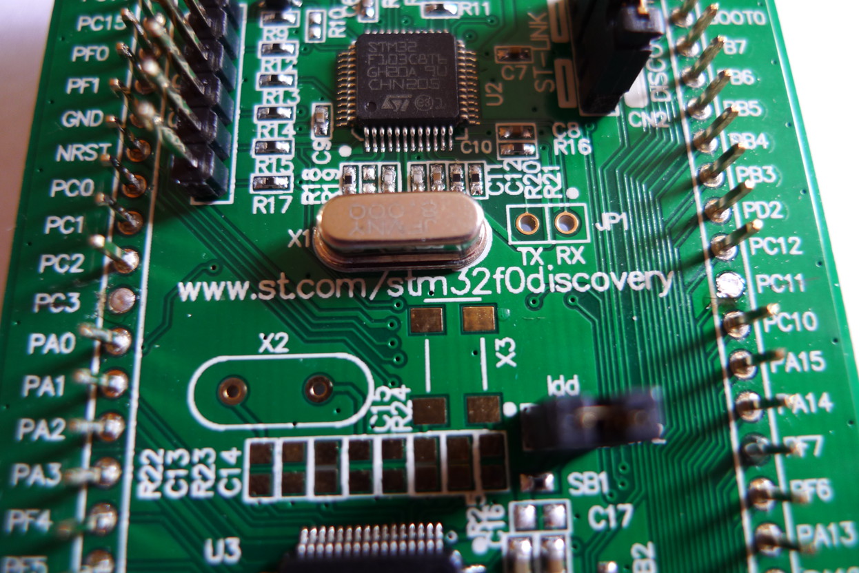
4. Tidy top board
The side 0.1” pin headers on the top board now don’t connect to anything (besides the 3.3V/5V/Gnd pins) and can be removed if desired. I also desoldered CN2 as that’s also unused.
You are now armed with a standalone ST-LINKv2 USB SWD device.
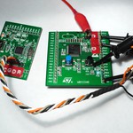
Bottom board
Since the top board contains the 3.3V regulator, you need to find some means of supplying 3.3V to the M0. Its Vcc is the right-hand pin of JP2 – remove the jumper. Ground is available still on the 0.1” headers at the side.
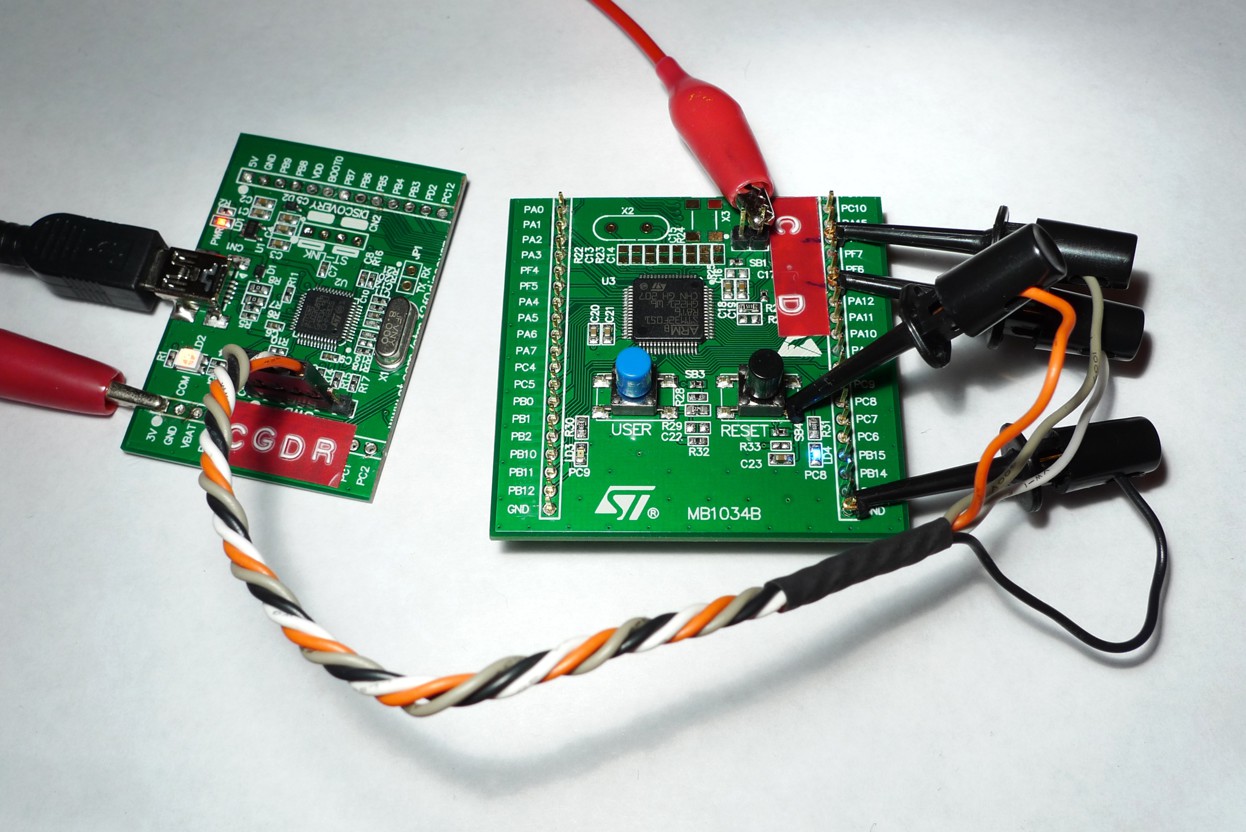
You need to clip your programmer wires onto the following pins to program the M0:
- PA13 for SWDIO
- PA14 for SWCLK
- nRESET – pick this up from the south-east leg of the reset switch
- GND
Should now be good to go. With a clippywire supplying 3.3V, you can see the separated board programming a ‘blinky blue LED’ routine into the Cortex-M0.
Software implications
In the Discovery Kit configuration, the CM3 is supplying an 8MHz clock to ‘HSI’ clock on the CM0. The CM0 starts up on its internal 8MHz RC oscillator so it’s safe not to have an external clock, but your software should configure the PLL to be driven from this internal ‘HSE’ clock instead of the external clock. Note the pads for crystals are still available (if you sawed carefully) so they are another option.
Going further
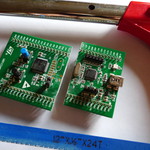
What if you have more than one of these boards? I bought two…
It would be cool if we could program the TOP microcontroller too; the STM32F103C8T6 72MHz Cortex-M3 is really pretty powerful, has a good amount of RAM and lots of flash. There’s also, obviously, the USB socket and circuitry!
Grab yourself the schematics of the STM32F0DK and have a look at what’s pinned out.
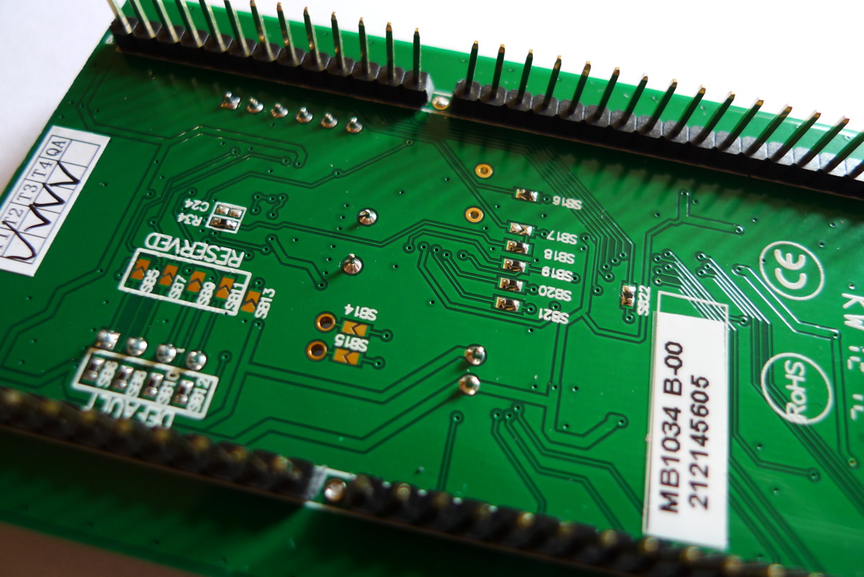
So if, from an earlier chop, we have an ST-LINK programmer with flyleads and clips (as shown here) how do we program another top-half? The solder bridges listed below make it easy. Check this on the schematic to make sure your revision is the same as mine…
- Undo solder bridges SB12 and SB8
- Bridge SB11 and SB7; SWDIO is now on CN2 pin 4 and SWCLK is pin 2
- Find nRESET: it is one half of SB13 (the other is ground)
- For ease, undoing SB6 will free up CN2 pin 1 – a little wire to connect SB13’s pad to put nRESET on pin 1 should let you program the chip solely from connections on CN2. (Pin 3 is ground.)
Many pins haven’t been wired out. These can be soldered to with thin wire, a soothing beer, a good iron and lots of flux and ventilation. There are also a few ‘easy’ IOs that are pinned out to something else on the board, so you can pick them up with slightly-larger-soldering:
| Pin | Where |
|---|---|
| PA0 | Remove R20/R21 and use their pads to access |
| PA2,PA3 | UART available on JP1 header |
| PA5 | T_JTCK, available on CN3 pin 2 |
| PA7 | T_NRST, available on CN3 pin 5 |
| PA8 | Remove R34, use its pad to access |
| PA10 | T_SWO, available on CN3 pin 6 |
| PB12 | Remove R11 |
| PB14 | T_JTMS, CN3 pin 4 |
| PC13 | Remove R18, use pad |
| PC14 | R19’s pad (R not fitted) |
11 total, plus USB; note there’re analog pins available and the STM32F103 has dual ADCs capable of 1MHz sampling.
So, this just leaves me to say: Two useful boards for the price of one! Not bad for 7 quid. :D
Images:

-
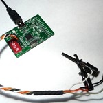
- Removed pins
-
- Chopped!
-
- Croc clips on standalone programmer

-
- Programming bottom half